Г
Л А В А 3. Статистика носителей заряда
в полупроводниках 149
Г
Л А В А 3
Кинетика носителей заряда
В
ПОЛУПРОВОДНИКАХ И ТОКИ
(диффузионные
и дрейфовые токи в полупроводниках и
переходах)
В
отсутствие внешних сил, например,
электрического поля, свободные носители
заряда в полупроводниках, как и в металлах
движутся хаотически, подобно молекулам
газа. Средняя скорость теплового
хаотического движения определяется
выражением
![]() ,
,
м/c,
где
k–постоянная Больцмана,Т–абсолютная температура,m– масса электрона.
При
своем движении электроны испытывают
столкновения из-за:
нарушения
периодичности потенциала внутреннего
электрического поля атомов и ионов под
действием тепловых колебаний решетки,
которые называются фононами;
дефектов
кристаллической решетки и примесей,
находящихся в кристалле;
взаимодействия
с другими носителями заряда.
При
этом средний ток носителей в любом
выбранном направлении равен нулю. Время
свободного пробега носителей tпочень мало и составляет величину 10-12с. Длина свободного пробега носителей
зарядаlправнаlп=vт·tп=105·10-12=10-7
м=0,1 мкм. Это составляет примерно 200
межатомных расстояний.
При
наличии сторонних сил в полупроводниках
может возникать направленное движение
зарядов, создающее электрический ток,
В зависимости от природы возбуждающей
силы в полупроводниках существует
дрейфовое и диффузионное движения
зарядов.
3.1. Подвижность. Дрейф носителей заряда
Если
в полупроводнике создано электрическое
поле величины Е, то помимо хаотического
появляется направленное перемещение
носителей заряда, называемоедрейфом.Скорость дрейфа,vдр,
– это скорость, направленная вдоль
вектора напряженности электрического
поля, усредненная по всем носителям
заряда одного знака (электронами или
дырками).
Оценить
среднюю скорость дрейфа можно исходя
из формулы vдр=a
tп, гдеа– ускорение, приобретаемое электроном
между столкновениями. Среднее ускорение
электрона можно рассчитать, используя
второй закон Ньютона
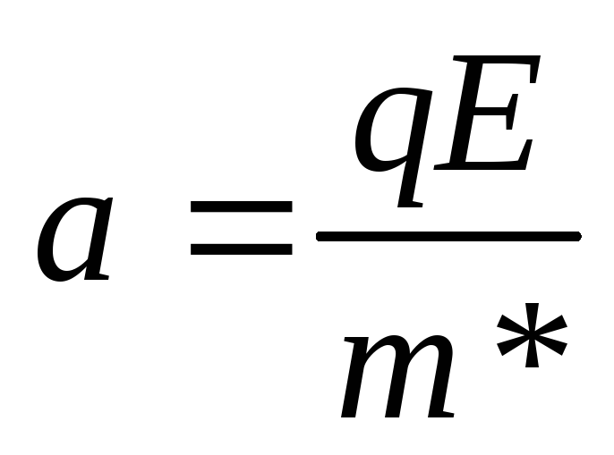 ,
,
где
qE=F– сила, действующая на электрон со
стороны поля.
Подставив
это выражение в формулу для скорости
дрейфа, получаем
![]() .
.
(3.1)
В
формуле (3.1) величина
![]() называетсяподвижностью носителей заряда.
называетсяподвижностью носителей заряда.
Таким образом, подвижность носителей
заряда обратно пропорциональна
эффективной массе носителейmи
прямо пропорциональна времени свободного
пробегаtп.
Поскольку
скорость дрейфа vдр=μЕ,
то значение подвижности можно рассчитать
по формуле
![]() ,
,
м2/В·с. (3.2)
Иначе
говоря, подвижность носителей заряда
– это скорость дрейфа, приобретаемая
свободными носителями в электрическом
поле напряженности Е=1 В/м.
Оценка
величины подвижности электрона μ в
кристаллической решетке по формуле
(3.1) дает следующее значение:
![]() м2/В·с.
м2/В·с.
Поскольку
в полупроводниках существуют два вида
носителей заряда с различными эффективными
массами, то различают подвижность
электронов nи подвижность дырокp.
Подвижность электронов в кремнии по
различным данным составляет (0,14…0,19)
м2/(Вс), а в
арсениде галлия – (0,93…1,1) м2/(Вс).
Подвижность дырок оказывается значительно
меньшей и равной (0,04…0,05) м2/(Вс)
для кремния и германия и 0,045 м2/(Вс)
для арсенида галлия, что объясняется
меньшим временем свободного пробега
дырок в этих полупроводниковых материалах.
Соседние файлы в папке лекции по ФОМЭ
- #
- #
- #
- #
- #
- #
- #
- #
- #
- #
- #
На заряженную частицу (электрон, дырку), движущуюся в электрическом $vec E$ и магнитном $vec B$ полях, действует сила Лоренца
$$
vec F = m^* ddot{vec r} = qvec E + frac{q}{c} [vec v times vec B]
$$
в СГС, а в СИ:
$$
vec F = m^* ddot{vec r} = qvec E + q[vec v times vec B]
$$
где $m^{*}$ — эффективная масса заряженной частицы, учитывающая влияние периодического поля на движение частицы в веществе, $c$ — скорость света; $q$ — заряд частицы; $vec v$ — скорость частицы; $ddot{{vec r}}$ — ускорение частицы.
Если пренебречь столкновениями движущейся частицы, то траекторию движения ее в электрическом и магнитном полях под действием силы Лоренца можно найти по этому уравнению.
Рассмотрим кратко характер движения свободного носителя заряда при наличии электрического и магнитного полей.
Под действием электрической составляющей поля частица получает дополнительную скорость, совпадающую с направлением вектора ${vec E}$. В общем случае при любой ориентации скорости ${vec v}$ и магнитного поля ${vec B}$ скорость электрона можно разложить на две составляющие: параллельную $v_{parallel } $ и перпендикулярную $v_{bot } $ полю ${vec B}$:
$$
vec v = (v_{parallel },v_{bot });
$$
тогда сила, действующая на частицу в магнитном поле,
$$
F_{B} =frac{qv_{bot } B}{c} .
$$
Сила ${vec F}_{B} $ все время изменяет направление скорости $v_{bot },$ тогда как $v_{parallel } $ остается постоянной и заставляет двигаться заряженную частицу по винтовой линии вдоль магнитного поля. При $v_{parallel } =0$ заряженная частица будет вращаться по окружности радиуса
$$
r=cfrac{m^{*} cdot v_{bot } }{qcdot B}
$$
с угловой скоростью
$$
omega =frac{qcdot B}{m^{*} c} .
$$
Если электрическое и магнитное поля параллельны, то заряженная частица движется по винтовой линии с непрерывно возрастающим шагом, поскольку электрическое поле меняет скорость ${bf v}_{parallel } $ и не влияет на ${bf v}_{bot }.$
Если электрическое и магнитное поля перпендикулярны (скрещенные поля), то при начальной скорости движения заряженной частицы, равной нулю, решение уравнения движения частицы под действием силы Лоренца дает уравнение циклоиды: частица вращается по окружности радиуса $r$, а центр окружности движется равномерно в направлении, перпендикулярном электрическому и магнитному полю со скоростью дрейфа
$$
{vec v}_{д}= frac{c}{B^2}cdot [vec Etimes vec B].
$$
Амплитуда периодического движения совпадает с Ларморовским радиусом $rho _{L} =frac{v_{bot }}{omega _{c} }$. Отметим, что это справедливо для свободной частицы, которая не сталкивается с другими частицами и с какими-либо другими объектами.
Рассмотрим поведение частицы с учётом столкновений частиц. Из курса молекулярной физики известно, что все частицы совершают хаотическое тепловое движение. Важной характеристикой такого движения является средняя длина свободного пролёта — $langle lrangle $. Зная среднюю (по модулю) тепловую скорость, можно определить среднее время между столкновениями частиц $tau =frac{langle lrangle}{langle | v | rangle }$. Если на частицы не действует внешняя сила, то средняя проекция тепловой скорости на любое направление равна нулю. При наложении внешнего постоянного электрического поля на частицу будет действовать постоянная сила. Следовательно, в промежутках между столкновениями её движение является равноускоренным, и она приобретает дополнительный импульс и, следовательно, дополнительную скорость в направлении действия силы. Если добавка к скорости, которую частица приобретает вследствие действия электрического поля, за время $tau $ много меньше её средней по модулю тепловой скорости, то такое поле называется слабым. После столкновения частица равновероятно рассеивается в любом направлении, значит в среднем, проекция её скорости на любое направление равна нулю. Двигаясь далее, она опять испытывает ускорение, приобретает дополнительную скорость и так далее. Таким образом, частица, кроме хаотического теплового движения, совершает дрейф с некоторой средней скоростью $v_{d}.$
В приближении слабого поля дрейфовая скорость $v_{d} $ много меньше средней по модулю тепловой скорости и время $tau $ не зависит от дрейфовой скорости и, соответственно, от внешней силы. Приобретаемый частицей дополнительный импульс и скорость пропорциональны как внешней силе $F_{E} $, так и времени действия этой силы $tau $. Таким образом, в слабом электрическом поле дрейфовая скорость пропорциональна напряжённости электрического поля ${vec v}_{d}=ucdot vec E$, где коэффициент пропорциональности $u$ называется подвижностью носителей заряда, в СИ подвижность имеет размерность $frac{м^2}{Вcdot с}$, но часто измеряется в несистемных единицах $frac{см^2}{Вcdot с}$.
Рассмотрим однородный изотропный полупроводник в форме параллелепипеда

Контакты 1 и 2 будем называть токовыми контактами, контакты 3 и 4 — потенциальными контактами. В отсутствие магнитного поля, если образец однороден и изотропен, контакты 3 и 4 находятся на эквипотенциальной поверхности и при пропускании тока через образец, падение напряжения между контактами 3 и 4 равно нулю. Поместим наш образец в однородное магнитное поле, вектор магнитного поля $vec В$ перпендикулярен вектору $vec j$. Скорость движения заряженных частиц состоит из хаотической (тепловой) и дрейфовой составляющих. Дрейфовая скорость возникает вследствие действия на заряженную частицу внешних сил (в нашем случае из-за приложенных внешних электрического и магнитного полей $vec E$ и $vec B$). В силу линейности зависимости силы Лоренца от скорости имеем:
$$
vec F = qvec E + frac{q}{c} [{vec v}_T times vec B]+frac{q}{c} [{vec v}_d times vec B],
$$
Так как средняя проекция тепловой скорости на любую ось равна нулю, то при усреднении второе слагаемое в последней формуле становится равным нулю, и средняя сила зависит только от дрейфовой скорости. Видно, что магнитная составляющая силы Лоренца отклоняет как положительно, так и отрицательно заряженные частицы в одну и ту же сторону, поскольку изменение знака заряда компенсируется изменением направления дрейфовой скорости на противоположную.
Предположим, что ток в образце определяется движением заряженных частиц одного типа, например, электронов (иначе придётся учитывать вклад в ток движение заряженных частиц всех типов). В отсутствие магнитного поля ток течёт слева направо. После включения магнитного поля, на электроны начинает действовать магнитная составляющая силы Лоренца, которая отклоняет их в направлении к грани 3. Таким образом, некоторое время после включения магнитного поля происходит движение электронов от грани 4 к грани 3. Электроны, создают на грани 3 отрицательный, а на грани 4 положительный заряды, то есть между этими гранями возникнет дополнительное электрическое поле ${vec E}_H$. Заряд на гранях 3 и 4 будет расти до тех пор, пока магнитная составляющая силы Лоренца не уравновесится этим дополнительным электрическим полем:
$$
ecdot {vec E}_y +frac ec [{vec v}_d times vec B] = 0.
$$
В этой ситуации имеем:
$
E_{y} =frac{v_{d}}{c} B.
$
Так как мы рассматриваем движение электрона за время свободного пробега, то ясно, что в формуле стоит средняя скорость дрейфа, определяемая средним по ансамблю электронов временем свободного пробега $langle tau rangle$ (средним временем релаксации). Поскольку
$$
j_{x} =-env_{d},
$$ то
$$
E_{y} =E_{H} =-frac{j_{x} B}{en}.
$$
Величина $E_H$ называется полем Холла. Таким образом, электрическое поле (для нашей ориентации векторов) имеет компоненты $E_x$ и $E_y$, следовательно, полный вектор электрического поля $vec E = vec i E_{x} + vec k E_{y}$ не будет совпадать по величине и направлению с первоначальным, (когда $vec{В}= 0$) между ними будет угол $varphi _H$, получивший название угол Холла. Для тангенса этого угла можно записать:
$$
tg (varphi _{H}) =frac{E_y}{E_x}
$$
или
$$
tg (varphi _{H}) =-frac{sigma B}{en}=-u_{n} B.
$$
На практике удобнее измерять не напряженность электрического поля, а соответствующую разность потенциалов (между гранями 3 и 4 на рисунке), которая называется ЭДС Холла:
$$
U_{H} =E_{H} cdot d=-frac{j_{x} Bd}{en}.
$$
Если выразить полный ток через плотность тока,
$I=j_{x} dcdot h$, то
$$
U_{H} =-frac{IB}{enh}=frac{R_{H} IB}{h},
$$
где $R_{H} =-(en)^{-1}$ — постоянная Холла.
В случае полупроводника р–типа проводимости в уравнении ($E_{y} =E_{H} =-frac{j_{x} B}{en}$) следует изменить знак носителей заряда с $-е$ на $+е$. Тогда будем иметь:
$$
E_{H}=frac{j_{x} B}{ep}=j_{x} R_{H} B,
$$
$$
tg (varphi _{H})=-frac{sigma B}{ep}=-u_{p} B,
$$
$$U_{H} =-frac{IB}{eph}=frac{R_{H} IB}{h},
$$
где р — концентрация дырок, $u_p$ — их подвижность, $R_H = (e p)^{-1}$ — постоянная Холла для дырочного полупроводника. Сопоставляя последние формулы, можно видеть, что по знаку эдс Холла можно определить в эксперименте тип носителей заряда, а по величине $R_H$ — их концентрацию. Кроме того, если возможно измерение и проводимости, и постоянной Холла, то по ним определяют подвижность носителей:
$$
u_{n(p)} =sigma R_{H} .
$$
Исследование эффекта Холла в полупроводниках осложняется тем, что в них существует несколько типов носителей зарядов. Проводимость, обусловленная движением одинакового количества электронов и дырок, называется собственной. Обычно полупроводники обладают примесной проводимостью. В полупроводниках такого типа некоторые атомы основного кристалла заменены атомами другой валентности. Если валентность атомов примеси больше, чем у основного кристалла, то у атома примеси есть «лишний» электрон, слабо связанный с атомным остовом, который он может легко отдать в зону проводимости. В таком полупроводнике больше электронов, чем дырок, он называется полупроводником n–типа, и обладает электронной проводимостью. При обратном соотношении валентностей основных и примесных атомов реализуется проводимость p–типа (дырочная). В полупроводниках могут также присутствовать оба типа носителей заряда.
Теперь рассмотрим ситуацию, когда в полупроводнике есть и электроны, и дырки. Запишем общий вид уравнений движения для электронов и дырок в электрическом и магнитном полях:
$$
m frac{d{vec v}_n}{dt} =-evec E- frac{e}{c}[{vec v}_n vec B] mbox{ — для электронов, }
m frac{d{vec v}_p}{dt} =-evec E- frac{e}{c}[{vec v}_p vec B] mbox{ — для дырок.}
$$
Проинтегрировав эти уравнения, и используя соотношение для подвижности $u_n =frac{e langle tau rangle}{m_n}$, получим:
$$
vec v_{n(p)} =-u_{n(p)} vec E-frac{u_{n(p)}^2}{c} [vec E times vec B],
$$
Помножив первое уравнение на $en$, а второе на $ep$, получим уравнения для электронного и дырочного токов:
$$
vec j_{n(p)} =-en(p)u_{n(p)} vec E-en(p)frac{u_{n(p)}^2}{c} [vec E times vec B].
$$
Таким образом, полный ток:
$$
vec j =e(nu_n + pu_p) vec E+efrac{nu_n^2+pu_p^2}{c} [vec E times vec B]
$$
или в скалярной форме:
$$
j_x =e(nu_n + pu_p) E_x+efrac{nu_n^2+pu_p^2}{c} E_y B_z=j,
$$
$$
j_y =e(nu_n + pu_p) E_y+efrac{nu_n^2+pu_p^2}{c} E_x B_z=0.
$$
Поскольку магнитное поле слабое, то второе слагаемое в первом уравнении системы много меньше первого. С учетом этого, решив систему относительно $E_y$ , получим
$$
E_{H}=R_{H} jB,
$$
$$
R_{H} =frac{pu_{p}^{2} -nu_{n}^{2}}{e(nu_{n} +pu_{p})^2}.
$$
Из этого выражения видно, что при $n gg p$: $R_H = (en)^{-1}$, а при $pgg n$: $R_H = (ep)^{-1}$. В случае собственного полупроводника, где $n = p = n_i$,
$$
R_{H}=frac{u_{p} -u_{n}}{en_{i}(u_{n} +u_{p} )}=frac{1-b}{en_{i}(1+b)},
$$
где $b = frac{u_n}{u_p}$. Согласно последней формуле $R_H<0$ при $b>1$ (т.е. $u_n>u_p$) и $R_H>0$ при $b<1$ (т.е. $u_n<u_p$).
Выше мы полагали, что все носители заряда имеют одно и то же время релаксации, иными словами — мы считали вероятность рассеяния независящей от скорости движения. При строгом рассмотрении необходимо учитывать распределение носителей по скоростям; следствием этого будет зависимость времени релаксации электронов (дырок) от их кинетической энергии. Описание кинетических явлений в ансамбле частиц при учете их распределения по энергии обычно выполняют с помощью кинетического уравнения Больцмана. Следствием рассмотрения эффекта Холла с помощью этого уравнения будет появление множителя $r$
$$
r=frac{langle tau ^{2} rangle}{{langle tau rangle}^{2}}
$$
в выражении для постоянной Холла:
$$
R_{H} =-r(en)^{-1} mbox{ — для электронов, } R_{H} =-r(ep)^{-1} mbox{ — для дырок,}
$$
$$
R_{H}=frac re frac{pu_{p}^{2} -nu_{n}^{2} }{(nu_{n} +pu_{p})^{2}} mbox{ — для биполярной проводимости.}
$$
Здесь $langle tau rangle$ — среднее время релаксации, $langle tau ^{2} rangle$ — средний квадрат времени релаксации. Соответственно все полученные выше формулы, где есть множители $(en)^{-1}$ или $(ep)^{-1}$, верны с точностью до множителя $r$; в частности, для подвижности:
$$
u_{n}^{H} =frac{rsigma}{en}=ru_{n};
u_{p}^{H} = frac{rsigma}{ep}=ru_{p} .
$$
Поэтому подвижность, определяемую с помощью эффекта Холла, называют холловской, в отличие от истинной (дрейфовой). Множитель r получил название фактора Холла.
Поскольку $r$ определяется временем релаксации $tau$, то его величина будет зависеть от механизмов рассеяния носителей заряда. Подсчитано, что при рассеянии на акустических колебаниях кристаллической решетки $r= frac 38 pi approx 1,18,$ а при рассеянии на примесных ионах $r = 1,93.$ При низких температурах (для Ge $T < 250$ K, для Si $T < 100$ K) обычно доминирует рассеяние носителей на ионах примесей, а при высоких температурах (для Ge и Si — в том числе и при комнатной температуре) преобладает рассеяние на колебаниях решетки.
Как отмечалось выше, полученные нами результаты справедливы для случая слабого магнитного поля. Поскольку $tau = frac{langle lambda rangle}{langle vrangle}$, то соотношение между длиной свободного пробега $langle lambda rangle$ носителя заряда и радиусом его круговой орбиты в магнитном поле можно заменить на следующее:
$$
tau ll T=frac{2pi}{omega _{c}} mbox{ — для слабого поля,}
$$
$$
tau gg T=frac{2pi}{omega _{c}}$ mbox{ — для сильного поля,}
$$
где $T$ — период вращения частицы, $omega _{c}$ — циклотронная частота (частота вращения носителя заряда по круговой траектории в магнитном поле с индукцией $vec В$). Поскольку $omega = frac{qcdot B}{m^{*}}$, то подставив $omega _{c}$ в выражение выше, получим:
$$
frac{tau omega _{c}}{2pi} = frac{uB}{2pi} ll 1 mbox{ — для слабого поля, }$$
$$
frac{tau omega _{c}}{2pi} =frac{uB}{2pi} gg 1 mbox{ — для сильного поля. }$$
Приведенное определение сильного и слабого полей является классическим. Здесь не учитывается изменение энергетического спектра электрона в магнитном поле.
Назад к Подвижность и коэффициент диффузии носителей заряда в полупроводниках, далее Приложение 1. Эффект Холла в сильном магнитном поле (для дополнительного чтения)
Подвижность носителей заряда — коэффициент пропорциональности между дрейфовой скоростью носителей и приложенным внешним электрическим полем. Определяет способность электронов и дырок в металлах и полупроводниках реагировать на внешнее воздействие. Размерность подвижности м2/(В·с) или см2/(В·с). Фактически подвижность численно равна средней скорости носителей заряда при напряженности электрического поля в 1 В/м. Стоит заметить, что мгновенная скорость может быть много больше дрейфовой. Понятие подвижности может применяться только при слабых электрических полях, когда выполняется линейность по электрическому полю и нет разогрева носителей, которое связано с квадратом электрического поля.
Содержание
- 1 Однородная среда
- 2 Тензорная запись
- 3 Холловская подвижность
- 4 Поверхностная подвижность
- 5 Примечания
Однородная среда
В простейшем случае изотропной среды в качестве определения подвижности (данного типа носителей тока) можно записать:

где  — абсолютная величина дрейфовой скорости (средней скорости дрейфа носителей под действием данного поля), а
  — абсолютная величина напряженности этого поля (важно, что
  неотрицательно даже при дрейфе носителей против поля — когда они отрицательно заряжены).
В случае однородной среды, не зависит от положения (внутри данной среды).
Дрейфовая скорость вместе с концентрацией носителей тока определяют ток (плотность тока) в среде:

И подвижность таким образом связана с проводимостью среды

и, соответственно, с ее удельным сопротивлением:

(Эти формулы написаны для случая, когда электропроводность обусловлена одним типом носителей; в противном случае нужно суммировать по всем типам носителей:

— впрочем, во многих случаях один из типов носителей дает подавляющий вклад, тогда можно приближенно пользоваться формулой для единственного носителя, имея в виду этот главный тип).
В классических моделях, таких, как модель Друде, (достаточно хороших почти во всех отношениях в случае твердого тела лишь для описания массивных носителей со сравнительно малой подвижностью, например, ионов, но не для электронов в металле), дрейфовая скорость имеет порядок действительной скорости движения носителей. Для случаев же, подобных случаю электронов проводимости в металле, имеющих модуль скорости порядка скорости Ферми, дрейфовая скорость, гораздо меньшая, чем эта величина, на самом деле есть лишь векторное (с учетом знака) усреднение этих больших скоростей, с учетом концентрации, которая зависит от направления (см. Модель Лифшица); однако это ничуть не мешает формально использовать понимаемую так дрейфовую скорость так, как она используется в формулах здесь.
Для подвижности в классических моделях известно также следующее выражение, получаемое из кинетического уравнения Больцмана в приближении времени релаксации :

где  — эффективная масса носителей.
Тензорная запись
В анизотропной среде подвижность связывает компоненты дрейфовой скорости  с компонентами электрического поля

Холловская подвижность
Указанная выше подвижность носителей заряда также называется дрейфовой подвижностью  . Она отличается от холловской подвижности
  , которую можно определить с помощью эффекта Холла (см. Метод ван дер Пау).
 ,
,
где  — холл-фактор, — время релаксации носителей заряда. Холл-фактор является атрибутом реального твёрдого тела и зависит от механизма рассеяния носителей: при рассеянии на ионах примеси
  ; при рассеянии на фононах
  ; в металлах и сильно вырожденных полупроводниках, а также в сильном магнитном поле (
 )
)  [1].
[1].
Поверхностная подвижность
Поверхностной подвижностью называется подвижность носителей, движущихся параллельно поверхности в приповерхностной области твердого тела, связанная со специфическими механизмами рассеяния, вызванными наличием поверхности раздела двух фаз.
Примечания
- ↑ Кучис, Е. В. Методы исследования эффекта Холла. — Москва : Советское радио, 1974. — P. 11-12.
Дрейфовый ток, подвижность носителей зарядов

Схемотехника
В полупроводниках свободные электроны и дырки находятся в состоянии хаотического движения. Поэтому, если выбрать произвольное сечение внутри объема полупроводника и подсчитать число носителей зарядов, проходящих через это сечение за единицу времени слева направо и справа налево, значения этих чисел окажутся одинаковыми. Это означает, что электрический ток в данном объеме полупроводника отсутствует.
При помещении полупроводника в электрическое поле на хаотическое движение носителей зарядов накладывается составляющая направленного движения. Направленное движение носителей зарядов в электрическом поле обусловливает появление тока, называемого дрейфовым током. Из-за столкновения носителей зарядов с атомами кристаллической решетки их движение в направлении действия электрического поля будет прерывистым. Такое движение может быть охарактеризовано средней скоростью движения носителей зарядов в направлении действия электрического поля. Средняя скорость движения носителей зарядов в поле единичной напряженности называется подвижностью или коэффициентом подвижности носителей заряда.
Подвижность носителей заряда зависит от механизма их рассеяния в кристаллической решетке. Подвижности электронов ((mu_n)) и дырок ((mu_p)) в полупроводнике имеют различное значение ((mu_n > mu_p)) и определяются температурой и концентрацией примесей. Увеличение температуры приводит к уменьшению подвижности, что зависит от числа столкновений носителей зарядов в единицу времени.
Зная подвижность и концентрацию носителей зарядов в полупроводнике, можно легко определить его удельную электропроводность ((sigma)):
(sigma=sigma_n+sigma_p=qleft(nmu_n+pmu_pright)),
где (sigma_n) ,(sigma_p) — электронная и дырочная составляющие электропроводности,
(q) — элементарный отрицательный заряд,
(n) и (p) — концентрации, соответственно, электронов и дырок.
Для полупроводника с собственной электропроводностью:
(n = p = n_i ), (sigma_i=qn_ileft(mu_n+mu_pright)).
Для полупроводника (n)-типа:
(sigmaapproxsigma_n=qn_{n0}mu_n).
Для полупроводника (p)-типа:
(sigmaapproxsigma_p=qp_{p0}mu_p),
где (n_{n0}) и (p_{p0}) — концентрации электронов и дырок в полупроводнике
в состоянии теплового равновесия.
В области высоких температур концентрация свободных носителей в полупроводнике значительно возрастает из-за разрыва ковалентных связей и, несмотря на уменьшение их подвижности, электропроводность полупроводника увеличивается по экспоненциальному закону.
| < Предыдущая | Следующая > |
|---|
This article is about the mobility for electrons and holes in metals and semiconductors. For the general concept, see Electrical mobility.
In solid-state physics, the electron mobility characterises how quickly an electron can move through a metal or semiconductor when pulled by an electric field. There is an analogous quantity for holes, called hole mobility. The term carrier mobility refers in general to both electron and hole mobility.
Electron and hole mobility are special cases of electrical mobility of charged particles in a fluid under an applied electric field.
When an electric field E is applied across a piece of material, the electrons respond by moving with an average velocity called the drift velocity,  . Then the electron mobility μ is defined as

Electron mobility is almost always specified in units of cm2/(V⋅s). This is different from the SI unit of mobility, m2/(V⋅s). They are related by 1 m2/(V⋅s) = 104 cm2/(V⋅s).
Conductivity is proportional to the product of mobility and carrier concentration. For example, the same conductivity could come from a small number of electrons with high mobility for each, or a large number of electrons with a small mobility for each. For semiconductors, the behavior of transistors and other devices can be very different depending on whether there are many electrons with low mobility or few electrons with high mobility. Therefore mobility is a very important parameter for semiconductor materials. Almost always, higher mobility leads to better device performance, with other things equal.
Semiconductor mobility depends on the impurity concentrations (including donor and acceptor concentrations), defect concentration, temperature, and electron and hole concentrations. It also depends on the electric field, particularly at high fields when velocity saturation occurs. It can be determined by the Hall effect, or inferred from transistor behavior.
Introduction[edit]
Drift velocity in an electric field[edit]
Without any applied electric field, in a solid, electrons and holes move around randomly. Therefore, on average there will be no overall motion of charge carriers in any particular direction over time.
However, when an electric field is applied, each electron or hole is accelerated by the electric field. If the electron were in a vacuum, it would be accelerated to ever-increasing velocity (called ballistic transport). However, in a solid, the electron repeatedly scatters off crystal defects, phonons, impurities, etc., so that it loses some energy and changes direction. The final result is that the electron moves with a finite average velocity, called the drift velocity. This net electron motion is usually much slower than the normally occurring random motion.
The two charge carriers, electrons and holes, will typically have different drift velocities for the same electric field.
Quasi-ballistic transport is possible in solids if the electrons are accelerated across a very small distance (as small as the mean free path), or for a very short time (as short as the mean free time). In these cases, drift velocity and mobility are not meaningful.
Definition and units[edit]
The electron mobility is defined by the equation:

where:
- E is the magnitude of the electric field applied to a material,
- vd is the magnitude of the electron drift velocity (in other words, the electron drift speed) caused by the electric field, and
- µe is the electron mobility.
The hole mobility is defined by a similar equation:

Both electron and hole mobilities are positive by definition.
Usually, the electron drift velocity in a material is directly proportional to the electric field, which means that the electron mobility is a constant (independent of the electric field). When this is not true (for example, in very large electric fields), mobility depends on the electric field.
The SI unit of velocity is m/s, and the SI unit of electric field is V/m. Therefore the SI unit of mobility is (m/s)/(V/m) = m2/(V⋅s). However, mobility is much more commonly expressed in cm2/(V⋅s) = 10−4 m2/(V⋅s).
Mobility is usually a strong function of material impurities and temperature, and is determined empirically. Mobility values are typically presented in table or chart form. Mobility is also different for electrons and holes in a given material.
Derivation[edit]
Starting with Newton’s Second Law:

where:
- a is the acceleration between collisions.
- F is the electric force exerted by the electric field, and
 is the effective mass of an electron.

Since the force on the electron is −eE:

This is the acceleration on the electron between collisions. The drift velocity is therefore:

where  is the mean free time
Since we only care about how the drift velocity changes with the electric field, we lump the loose terms together to get

where 
Similarly, for holes we have

where 
Note that both electron mobility and hole mobility are positive. A minus sign is added for electron drift velocity to account for the minus charge.
Relation to current density[edit]
The drift current density resulting from an electric field can be calculated from the drift velocity. Consider a sample with cross-sectional area A, length l and an electron concentration of n. The current carried by each electron must be  , so that the total current density due to electrons is given by:

Using the expression for gives

A similar set of equations applies to the holes, (noting that the charge on a hole is positive). Therefore the current density due to holes is given by

where p is the hole concentration and  the hole mobility.
The total current density is the sum of the electron and hole components:

Relation to conductivity[edit]
We have previously derived the relationship between electron mobility and current density
Now Ohm’s Law can be written in the form

where  is defined as the conductivity. Therefore we can write down:

which can be factorised to

Relation to electron diffusion[edit]
In a region where n and p vary with distance, a diffusion current is superimposed on that due to conductivity. This diffusion current is governed by Fick’s Law:

where:
- F is flux.
- De is the diffusion coefficient or diffusivity
- is the concentration gradient of electrons

The diffusion coefficient for a charge carrier is related to its mobility by the Einstein relation:

where:
- kB is the Boltzmann constant
- T is the absolute temperature
- e is the electric charge of an electron
Examples[edit]
Typical electron mobility at room temperature (300 K) in metals like gold, copper and silver is 30–50 cm2/ (V⋅s). Carrier mobility in semiconductors is doping dependent. In silicon (Si) the electron mobility is of the order of 1,000, in germanium around 4,000, and in gallium arsenide up to 10,000 cm2/ (V⋅s). Hole mobilities are generally lower and range from around 100 cm2/ (V⋅s) in gallium arsenide, to 450 in silicon, and 2,000 in germanium.[1]
Very high mobility has been found in several ultrapure low-dimensional systems, such as two-dimensional electron gases (2DEG) (35,000,000 cm2/(V⋅s) at low temperature),[2] carbon nanotubes (100,000 cm2/(V⋅s) at room temperature)[3] and freestanding graphene (200,000 cm2/ V⋅s at low temperature).[4] Organic semiconductors (polymer, oligomer) developed thus far have carrier mobilities below 50 cm2/(V⋅s), and typically below 1, with well performing materials measured below 10.[5]
| Material | Electron mobility | Hole mobility |
|---|---|---|
| AlGaAs/GaAs heterostructures | 35,000,000[2] | |
| Freestanding Graphene | 200,000[4] | |
| Carbon nanotubes | 79,000[6][7] | |
| Cubic boron arsenide (c-BAs) | 1,600[8] | |
| Crystalline silicon | 1,400[1] | 450[1] |
| Polycrystalline silicon | 100 | |
| Metals (Al, Au, Cu, Ag) | 10-50 | |
| 2D Material (MoS2) | 10-50 | |
| Organics | 8.6[9] | 43[10] |
| Amorphous silicon | ~1[11] |
Electric field dependence and velocity saturation[edit]
At low fields, the drift velocity vd is proportional to the electric field E, so mobility μ is constant. This value of μ is called the low-field mobility.
As the electric field is increased, however, the carrier velocity increases sublinearly and asymptotically towards a maximum possible value, called the saturation velocity vsat. For example, the value of vsat is on the order of 1×107 cm/s for both electrons and holes in Si. It is on the order of 6×106 cm/s for Ge. This velocity is a characteristic of the material and a strong function of doping or impurity levels and temperature. It is one of the key material and semiconductor device properties that determine a device such as a transistor’s ultimate limit of speed of response and frequency.
This velocity saturation phenomenon results from a process called optical phonon scattering. At high fields, carriers are accelerated enough to gain sufficient kinetic energy between collisions to emit an optical phonon, and they do so very quickly, before being accelerated once again. The velocity that the electron reaches before emitting a phonon is:

where ωphonon(opt.) is the optical-phonon angular frequency and m* the carrier effective mass in the direction of the electric field. The value of Ephonon (opt.) is 0.063 eV for Si and 0.034 eV for GaAs and Ge. The saturation velocity is only one-half of vemit, because the electron starts at zero velocity and accelerates up to vemit in each cycle.[12] (This is a somewhat oversimplified description.[12])
Velocity saturation is not the only possible high-field behavior. Another is the Gunn effect, where a sufficiently high electric field can cause intervalley electron transfer, which reduces drift velocity. This is unusual; increasing the electric field almost always increases the drift velocity, or else leaves it unchanged. The result is negative differential resistance.
In the regime of velocity saturation (or other high-field effects), mobility is a strong function of electric field. This means that mobility is a somewhat less useful concept, compared to simply discussing drift velocity directly.
Relation between scattering and mobility[edit]
Recall that by definition, mobility is dependent on the drift velocity. The main factor determining drift velocity (other than effective mass) is scattering time, i.e. how long the carrier is ballistically accelerated by the electric field until it scatters (collides) with something that changes its direction and/or energy. The most important sources of scattering in typical semiconductor materials, discussed below, are ionized impurity scattering and acoustic phonon scattering (also called lattice scattering). In some cases other sources of scattering may be important, such as neutral impurity scattering, optical phonon scattering, surface scattering, and defect scattering.[13]
Elastic scattering means that energy is (almost) conserved during the scattering event. Some elastic scattering processes are scattering from acoustic phonons, impurity scattering, piezoelectric scattering, etc. In acoustic phonon scattering, electrons scatter from state k to k’, while emitting or absorbing a phonon of wave vector q. This phenomenon is usually modeled by assuming that lattice vibrations cause small shifts in energy bands. The additional potential causing the scattering process is generated by the deviations of bands due to these small transitions from frozen lattice positions.[14]
Ionized impurity scattering[edit]
Semiconductors are doped with donors and/or acceptors, which are typically ionized, and are thus charged. The Coulombic forces will deflect an electron or hole approaching the ionized impurity. This is known as ionized impurity scattering. The amount of deflection depends on the speed of the carrier and its proximity to the ion. The more heavily a material is doped, the higher the probability that a carrier will collide with an ion in a given time, and the smaller the mean free time between collisions, and the smaller the mobility. When determining the strength of these interactions due to the long-range nature of the Coulomb potential, other impurities and free carriers cause the range of interaction with the carriers to reduce significantly compared to bare Coulomb interaction.
If these scatterers are near the interface, the complexity of the problem increases due to the existence of crystal defects and disorders. Charge trapping centers that scatter free carriers form in many cases due to defects associated with dangling bonds. Scattering happens because after trapping a charge, the defect becomes charged and therefore starts interacting with free carriers. If scattered carriers are in the inversion layer at the interface, the reduced dimensionality of the carriers makes the case differ from the case of bulk impurity scattering as carriers move only in two dimensions. Interfacial roughness also causes short-range scattering limiting the mobility of quasi-two-dimensional electrons at the interface.[14]
Lattice (phonon) scattering[edit]
At any temperature above absolute zero, the vibrating atoms create pressure (acoustic) waves in the crystal, which are termed phonons. Like electrons, phonons can be considered to be particles. A phonon can interact (collide) with an electron (or hole) and scatter it. At higher temperature, there are more phonons, and thus increased electron scattering, which tends to reduce mobility.
Piezoelectric scattering[edit]
Piezoelectric effect can occur only in compound semiconductor due to their polar nature. It is small in most semiconductors but may lead to local electric fields that cause scattering of carriers by deflecting them, this effect is important mainly at low temperatures where other scattering mechanisms are weak. These electric fields arise from the distortion of the basic unit cell as strain is applied in certain directions in the lattice.[14]
Surface roughness scattering[edit]
Surface roughness scattering caused by interfacial disorder is short range scattering limiting the mobility of quasi-two-dimensional electrons at the interface. From high-resolution transmission electron micrographs, it has been determined that the interface is not abrupt on the atomic level, but actual position of the interfacial plane varies one or two atomic layers along the surface. These variations are random and cause fluctuations of the energy levels at the interface, which then causes scattering.[14]
Alloy scattering[edit]
In compound (alloy) semiconductors, which many thermoelectric materials are, scattering caused by the perturbation of crystal potential due to the random positioning of substituting atom species in a relevant sublattice is known as alloy scattering. This can only happen in ternary or higher alloys as their crystal structure forms by randomly replacing some atoms in one of the sublattices (sublattice) of the crystal structure. Generally, this phenomenon is quite weak but in certain materials or circumstances, it can become dominant effect limiting conductivity. In bulk materials, interface scattering is usually ignored.[14][15][16][17][18]
Inelastic scattering[edit]
During inelastic scattering processes, significant energy exchange happens. As with elastic phonon scattering also in the inelastic case, the potential arises from energy band deformations caused by atomic vibrations. Optical phonons causing inelastic scattering usually have the energy in the range 30-50 meV, for comparison energies of acoustic phonon are typically less than 1 meV but some might have energy in order of 10 meV. There is significant change in carrier energy during the scattering process. Optical or high-energy acoustic phonons can also cause intervalley or interband scattering, which means that scattering is not limited within single valley.[14]
Electron–electron scattering[edit]
Due to the Pauli exclusion principle, electrons can be considered as non-interacting if their density does not exceed the value 1016~1017 cm−3 or electric field value 103 V/cm. However, significantly above these limits electron–electron scattering starts to dominate. Long range and nonlinearity of the Coulomb potential governing interactions between electrons make these interactions difficult to deal with.[14][15][16]
Relation between mobility and scattering time[edit]
A simple model gives the approximate relation between scattering time (average time between scattering events) and mobility. It is assumed that after each scattering event, the carrier’s motion is randomized, so it has zero average velocity. After that, it accelerates uniformly in the electric field, until it scatters again. The resulting average drift mobility is:[19]

where q is the elementary charge, m* is the carrier effective mass, and τ is the average scattering time.
If the effective mass is anisotropic (direction-dependent), m* is the effective mass in the direction of the electric field.
Matthiessen’s rule[edit]
Normally, more than one source of scattering is present, for example both impurities and lattice phonons. It is normally a very good approximation to combine their influences using «Matthiessen’s Rule» (developed from work by Augustus Matthiessen in 1864):

where µ is the actual mobility,  is the mobility that the material would have if there was impurity scattering but no other source of scattering, and
  is the mobility that the material would have if there was lattice phonon scattering but no other source of scattering. Other terms may be added for other scattering sources, for example

Matthiessen’s rule can also be stated in terms of the scattering time:

where τ is the true average scattering time and τimpurities is the scattering time if there was impurity scattering but no other source of scattering, etc.
Matthiessen’s rule is an approximation and is not universally valid. This rule is not valid if the factors affecting the mobility depend on each other, because individual scattering probabilities cannot be summed unless they are independent of each other.[18] The average free time of flight of a carrier and therefore the relaxation time is inversely proportional to the scattering probability.[14][15][17] For example, lattice scattering alters the average electron velocity (in the electric-field direction), which in turn alters the tendency to scatter off impurities. There are more complicated formulas that attempt to take these effects into account.[20]
Temperature dependence of mobility[edit]
| Si | Ge | GaAs | |
|---|---|---|---|
| Electrons | ∝T −2.4 | ∝T −1.7 | ∝T −1.0 |
| Holes | ∝T −2.2 | ∝T −2.3 | ∝T −2.1 |
With increasing temperature, phonon concentration increases and causes increased scattering. Thus lattice scattering lowers the carrier mobility more and more at higher temperature. Theoretical calculations reveal that the mobility in non-polar semiconductors, such as silicon and germanium, is dominated by acoustic phonon interaction. The resulting mobility is expected to be proportional to T −3/2, while the mobility due to optical phonon scattering only is expected to be proportional to T −1/2. Experimentally, values of the temperature dependence of the mobility in Si, Ge and GaAs are listed in table.[21]
As  , where
  is the scattering cross section for electrons and holes at a scattering center and
  is a thermal average (Boltzmann statistics) over all electron or hole velocities in the lower conduction band or upper valence band, temperature dependence of the mobility can be determined. In here, the following definition for the scattering cross section is used: number of particles scattered into solid angle dΩ per unit time divided by number of particles per area per time (incident intensity), which comes from classical mechanics. As Boltzmann statistics are valid for semiconductors
  .
.
For scattering from acoustic phonons, for temperatures well above Debye temperature, the estimated cross section Σph is determined from the square of the average vibrational amplitude of a phonon to be proportional to T. The scattering from charged defects (ionized donors or acceptors) leads to the cross section  . This formula is the scattering cross section for «Rutherford scattering», where a point charge (carrier) moves past another point charge (defect) experiencing Coulomb interaction.
The temperature dependencies of these two scattering mechanism in semiconductors can be determined by combining formulas for τ, Σ and , to be for scattering from acoustic phonons  and from charged defects
  .[15][17]
The effect of ionized impurity scattering, however, decreases with increasing temperature because the average thermal speeds of the carriers are increased.[13] Thus, the carriers spend less time near an ionized impurity as they pass and the scattering effect of the ions is thus reduced.
These two effects operate simultaneously on the carriers through Matthiessen’s rule. At lower temperatures, ionized impurity scattering dominates, while at higher temperatures, phonon scattering dominates, and the actual mobility reaches a maximum at an intermediate temperature.
Disordered Semiconductors[edit]

While in crystalline materials electrons can be described by wavefunctions extended over the entire solid,[22] this is not the case in systems with appreciable structural disorder, such as polycrystalline or amorphous semiconductors. Anderson suggested that beyond a critical value of structural disorder,[23] electron states would be localized. Localized states are described as being confined to finite region of real space, normalizable, and not contributing to transport. Extended states are spread over the extent of the material, not normalizable, and contribute to transport. Unlike crystalline semiconductors, mobility generally increases with temperature in disordered semiconductors.
Multiple trapping and release[edit]
Mott later developed[24] the concept of a mobility edge. This is an energy  , above which electrons undergo a transition from localized to delocalized states. In this description, termed multiple trapping and release, electrons are only able to travel when in extended states, and are constantly being trapped in, and re-released from, the lower energy localized states. Because the probability of an electron being released from a trap depends on its thermal energy, mobility can be described by an Arrhenius relationship in such a system:
![]()
Energy band diagram depicting electron transport under multiple trapping and release.

where  is a mobility prefactor,
  is activation energy,
  is the Boltzmann constant, and
  is temperature. The activation energy is typically evaluated by measuring mobility as a function of temperature. The Urbach Energy can be used as a proxy for activation energy in some systems.[25]
Variable Range Hopping[edit]
At low temperature, or in system with a large degree of structural disorder (such as fully amorphous systems), electrons cannot access delocalized states. In such a system, electrons can only travel by tunnelling for one site to another, in a process called variable range hopping. In the original theory of variable range hopping, as developed by Mott and Davis,[26] the probability  , of an electron hopping from one site
  , to another site
  , depends on their separation in space
  , and their separation in energy
  .
.

Here  is a prefactor associated with the phonon frequency in the material,[27] and
  is the wavefunction overlap parameter. The mobility in a system governed by variable range hopping can be shown[26] to be:
![{displaystyle mu =mu _{0}exp left(-left[{frac {T_{0}}{T}}right]^{-1/(d+1)}right)}](https://wikimedia.org/api/rest_v1/media/math/render/svg/2ec6dbb01dae46490fe94780f7719b272fd5f4ad)
where is a mobility prefactor,  is a parameter (with dimensions of temperature) that quantifies the width of localized states, and
  is the dimensionality of the system.
Measurement of semiconductor mobility[edit]
Hall mobility[edit]

Hall effect measurement setup for holes

Hall effect measurement setup for electrons
Carrier mobility is most commonly measured using the Hall effect. The result of the measurement is called the «Hall mobility» (meaning «mobility inferred from a Hall-effect measurement»).
Consider a semiconductor sample with a rectangular cross section as shown in the figures, a current is flowing in the x-direction and a magnetic field is applied in the z-direction. The resulting Lorentz force will accelerate the electrons (n-type materials) or holes (p-type materials) in the (−y) direction, according to the right hand rule and set up an electric field ξy. As a result there is a voltage across the sample, which can be measured with a high-impedance voltmeter. This voltage, VH, is called the Hall voltage. VH is negative for n-type material and positive for p-type material.
Mathematically, the Lorentz force acting on a charge q is given by
For electrons:

For holes:

In steady state this force is balanced by the force set up by the Hall voltage, so that there is no net force on the carriers in the y direction. For electrons,
![{displaystyle {vec {F}}_{y}=(-q){vec {xi }}_{y}+(-q)[{vec {v}}_{n}times {vec {B}}_{z}]=0}](https://wikimedia.org/api/rest_v1/media/math/render/svg/ddcbe1f951022700b2af8e0537cebaa8bc411b4f)


For electrons, the field points in the −y direction, and for holes, it points in the +y direction.
The electron current I is given by  . Sub vx into the expression for ξy,

where RHn is the Hall coefficient for electron, and is defined as

Since 

Similarly, for holes

From the Hall coefficient, we can obtain the carrier mobility as follows:

Similarly,

Here the value of VHp (Hall voltage), t (sample thickness), I (current) and B (magnetic field) can be measured directly, and the conductivities σn or σp are either known or can be obtained from measuring the resistivity.
Field-effect mobility[edit]
The mobility can also be measured using a field-effect transistor (FET). The result of the measurement is called the «field-effect mobility» (meaning «mobility inferred from a field-effect measurement»).
The measurement can work in two ways: From saturation-mode measurements, or linear-region measurements.[28] (See MOSFET for a description of the different modes or regions of operation.)
Using saturation mode[edit]
In this technique,[28] for each fixed gate voltage VGS, the drain-source voltage VDS is increased until the current ID saturates. Next, the square root of this saturated current is plotted against the gate voltage, and the slope msat is measured. Then the mobility is:

where L and W are the length and width of the channel and Ci is the gate insulator capacitance per unit area. This equation comes from the approximate equation for a MOSFET in saturation mode:

where Vth is the threshold voltage. This approximation ignores the Early effect (channel length modulation), among other things. In practice, this technique may underestimate the true mobility.[29]
Using the linear region[edit]
In this technique,[28] the transistor is operated in the linear region (or «ohmic mode»), where VDS is small and  with slope mlin. Then the mobility is:

This equation comes from the approximate equation for a MOSFET in the linear region:

In practice, this technique may overestimate the true mobility, because if VDS is not small enough and VG is not large enough, the MOSFET may not stay in the linear region.[29]
Optical mobility[edit]
Electron mobility may be determined from non-contact laser photo-reflectance technique measurements. A series of photo-reflectance measurements are made as the sample is stepped through focus. The electron diffusion length and recombination time are determined by a regressive fit to the data. Then the Einstein relation is used to calculate the mobility.[30][31]
Terahertz mobility[edit]
Electron mobility can be calculated from time-resolved terahertz probe measurement.[32][33] Femtosecond laser pulses excite the semiconductor and the resulting photoconductivity is measured using a terahertz probe, which detects changes in the terahertz electric field.
Time resolved microwave conductivity (TRMC)[edit]
A proxy for charge carrier mobility can be evaluated using time-resolved microwave conductivity (TRMC).[35] A pulsed optical laser is used to create electrons and holes in a semiconductor, which are then detected as an increase in photoconductance. With knowledge of the sample absorbance, dimensions, and incident laser fluence, the parameter  can be evaluated, where
  is the carrier generation yield (between 0 and 1),
  is the electron mobility and is the hole mobility.
  has the same dimensions as mobility, but carrier type (electron or hole) is obscured.
Doping concentration dependence in heavily-doped silicon[edit]
The charge carriers in semiconductors are electrons and holes. Their numbers are controlled by the concentrations of impurity elements, i.e. doping concentration. Thus doping concentration has great influence on carrier mobility.
While there is considerable scatter in the experimental data, for noncompensated material (no counter doping) for heavily doped substrates (i.e.  and up), the mobility in silicon is often characterized by the empirical relationship:[36]

where N is the doping concentration (either ND or NA), and Nref and α are fitting parameters. At room temperature, the above equation becomes:
Majority carriers:[37]


Minority carriers:[38]


These equations apply only to silicon, and only under low field.
See also[edit]
- Speed of electricity
References[edit]
- ^ a b c «NSM Archive — Physical Properties of Semiconductors». www.matprop.ru. Retrieved 2020-07-25.
- ^ a b Umansky, V.; Heiblum, M.; Levinson, Y.; Smet, J.; Nübler, J.; Dolev, M. (2009). «MBE growth of ultra-low disorder 2DEG with mobility exceeding 35×106 cm2 V−1 s−1». Journal of Crystal Growth. 311 (7): 1658–1661. Bibcode:2009JCrGr.311.1658U. doi:10.1016/j.jcrysgro.2008.09.151.
- ^ Dürkop, T.; Getty, S. A.; Cobas, Enrique; Fuhrer, M. S. (2004). «Extraordinary Mobility in Semiconducting Carbon Nanotubes». Nano Letters. 4 (1): 35. Bibcode:2004NanoL…4…35D. doi:10.1021/nl034841q. S2CID 45010238.
- ^ a b Bolotin, K; Sikes, K; Jiang, Z; Klima, M; Fudenberg, G; Hone, J; Kim, P; Stormer, H (2008). «Ultrahigh electron mobility in suspended graphene». Solid State Communications. 146 (9): 351–355. arXiv:0802.2389. Bibcode:2008SSCom.146..351B. doi:10.1016/j.ssc.2008.02.024. S2CID 118392999.
- ^ Nawrocki, Robert (2016). «300‐nm Imperceptible, Ultraflexible, and Biocompatible e‐Skin Fit with Tactile Sensors and Organic Transistors». Advanced Electronic Materials. 2 (4): 1500452. doi:10.1002/aelm.201500452. S2CID 138355533.
- ^ Dürkop, T.; Getty, S. A.; Cobas, Enrique; Fuhrer, M. S. (2004). «Extraordinary Mobility in Semiconducting Carbon Nanotubes». Nano Letters. 4 (1): 35–39. Bibcode:2004NanoL…4…35D. doi:10.1021/nl034841q. S2CID 45010238.
- ^ Snow, E. S.; Campbell, P. M.; Ancona, M. G.; Novak, J. P. (2005). «High-mobility carbon-nanotube thin-film transistors on a polymeric substrate». Applied Physics Letters. 86 (3): 033105. Bibcode:2005ApPhL..86c3105S. doi:10.1063/1.1854721. ISSN 0003-6951. Archived from the original on September 24, 2017.
- ^ Shin, Jungwoo; Gamage, Geethal Amila; Ding, Zhiwei; Chen, Ke; Tian, Fei; Qian, Xin; Zhou, Jiawei; Lee, Hwijong; Zhou, Jianshi; Shi, Li; Nguyen, Thanh; Han, Fei; Li, Mingda; Broido, David; Schmidt, Aaron; Ren, Zhifeng; Chen, Gang (2022). «High ambipolar mobility in cubic boron arsenide». Science. 377 (6604): 437–440. Bibcode:2022Sci…377..437S. doi:10.1126/science.abn4290. PMID 35862526. S2CID 250952849.
- ^ He, Tao; Stolte, Matthias; Würthner, Frank (2013-12-23). «Air‐Stable n‐Channel Organic Single Crystal Field‐Effect Transistors Based on Microribbons of Core‐Chlorinated Naphthalene Diimide». Advanced Materials. 25 (48): 6951–6955. Bibcode:2013AdM….25.6951H. doi:10.1002/adma.201303392. PMID 24105872.
- ^ Yuan, Yongbo (2014). «Ultra-high mobility transparent organic thin film transistors grown by an off-centre spin-coating method». Nature Communications. 5: 3005. Bibcode:2014NatCo…5.3005Y. doi:10.1038/ncomms4005. PMID 24398476.
- ^ Heremans, Paul (2015). «Mechanical and Electronic Properties of Thin‐Film Transistors on Plastic, and Their Integration in Flexible Electronic Applications». Advanced Materials. 28 (22): 4266–4282. doi:10.1002/adma.201504360. PMID 26707947. S2CID 25457390.
- ^ a b Vladimir Vasilʹevich Mitin; Vi︠a︡cheslav Aleksandrovich Kochelap; Michael A. Stroscio (1999). Quantum heterostructures: microelectronics and optoelectronics. Cambridge University Press. pp. 307–9. ISBN 978-0-521-63635-3. Retrieved 2 March 2011.
- ^ a b Singh (2008). Electronic Devices And Integrated Circuits. PHI Learning Pvt. Ltd. pp. 77–. ISBN 978-81-203-3192-1. Retrieved 1 March 2011.
- ^ a b c d e f g h Ferry, David K. Semiconductor transport. London: Taylor & Francis, 2000. ISBN 0-7484-0865-7 (hbk.), ISBN 0-7484-0866-5 (pbk.)
- ^ a b c d Ibach, Harald. ; Luth, Hans. Solid-state physics : an introduction to principles of materials science / Harald Ibach, Hans Luth. New York: Springer, 2009. -(Advanced texts in physics) ISBN 978-3-540-93803-3
- ^ a b Bulusu, A. (2008). «Review of electronic transport models for thermoelectric materials». Superlattices and Microstructures. 44 (1): 1–36. Bibcode:2008SuMi…44….1B. doi:10.1016/j.spmi.2008.02.008..
- ^ a b c Bhattacharya, Pallab. Semiconductor optoelectronic devices / Pallab Bhattacharya. Upper Saddle River (NJ): Prentice-Hall, 1997. ISBN 0-13-495656-7 (nid.)
- ^ a b Y. Takeda and T.P. Pearsall, «Failure of Mattheissen’s Rule in the Calculation of Carrier Mobility and Alloy Scattering Effects in Ga0.47In0.53As», Electronics Lett. 17, 573-574 (1981).
- ^ Peter Y. Yu; Manuel Cardona (30 May 2010). Fundamentals of Semiconductors: Physics and Materials Properties. Springer. pp. 205–. ISBN 978-3-642-00709-5. Retrieved 1 March 2011.
- ^ Antonio Luque; Steven Hegedus (9 June 2003). Handbook of photovoltaic science and engineering. John Wiley and Sons. p. 79, eq. 3.58. ISBN 978-0-471-49196-5. Retrieved 2 March 2011. weblink (subscription only)
- ^ a b Chapter 2: Semiconductor Fundamentals. Online textbook by B. Van Zeghbroeck]
- ^ Hook, J. R.; Hall, H. E. (1991-09-05). Solid State Physics. Wiley. ISBN 978-0-471-92804-1.
- ^ Anderson, P. W. (1958-03-01). «Absence of Diffusion in Certain Random Lattices». Physical Review. 109 (5): 1492–1505. Bibcode:1958PhRv..109.1492A. doi:10.1103/PhysRev.109.1492.
- ^ Mott, N. F. (1967-01-01). «Electrons in disordered structures». Advances in Physics. 16 (61): 49–144. Bibcode:1967AdPhy..16…49M. doi:10.1080/00018736700101265. ISSN 0001-8732.
- ^ Brotherton, S. D. (2013). Introduction to Thin Film Transistors: Physics and Technology of TFTs. Springer International Publishing. p. 143. ISBN 978-3-319-00001-5.
- ^ a b Electronic Processes in Non-Crystalline Materials. Oxford Classic Texts in the Physical Sciences. Oxford, New York: Oxford University Press. 2012-03-24. ISBN 978-0-19-964533-6.
- ^ Emin, David (1974-02-11). «Phonon-Assisted Jump Rate in Noncrystalline Solids». Physical Review Letters. 32 (6): 303–307. Bibcode:1974PhRvL..32..303E. doi:10.1103/PhysRevLett.32.303.
- ^ a b c Constance Rost-Bietsch (August 2005). Ambipolar and Light-Emitting Organic Field-Effect Transistors. Cuvillier Verlag. pp. 17–. ISBN 978-3-86537-535-3. Retrieved 1 March 2011.. This reference mistakenly leaves out a factor of 1/VDS in eqn (2.11). The correct version of that equation can be found, e.g., in Stassen, A. F.; De Boer, R. W. I.; Iosad, N. N.; Morpurgo, A. F. (2004). «Influence of the gate dielectric on the mobility of rubrene single-crystal field-effect transistors». Applied Physics Letters. 85 (17): 3899–3901. arXiv:cond-mat/0407293. Bibcode:2004ApPhL..85.3899S. doi:10.1063/1.1812368. S2CID 119532427.
- ^ a b Constance Rost-Bietsch (August 2005). Ambipolar and Light-Emitting Organic Field-Effect Transistors. Cuvillier Verlag. pp. 19–. ISBN 978-3-86537-535-3. Retrieved 20 April 2011. «Extracting the field-effect mobility directly from the linear region of the output characteristic may yield larger values for the field-effect mobility than the actual one, since the drain current is linear only for very small VDS and large VG. In contrast, extracting the field-effect mobility from the saturated region might yield rather conservative values for the field-effect mobility, since the drain-current dependence from the gate-voltage becomes sub-quadratic for large VG as well as for small VDS.»
- ^ W. Chism, «Precise Optical Measurement of Carrier Mobilities Using Z-scanning Laser Photoreflectance,» arXiv:1711.01138 [physics:ins-det], Oct. 2017.
- ^ W. Chism, «Z-scanning Laser Photoreflectance as a Tool for Characterization of Electronic Transport Properties,» arXiv:1808.01897 [cond-mat:mes-hall], Aug. 2018.
- ^ Ulbricht, Ronald; Hendry, Euan; Shan, Jie; Heinz, Tony F.; Bonn, Mischa (2011). «Carrier dynamics in semiconductors studied with time-resolved terahertz spectroscopy» (PDF). Reviews of Modern Physics. 83 (2): 543–586. Bibcode:2011RvMP…83..543U. doi:10.1103/RevModPhys.83.543. hdl:10871/15671. ISSN 0034-6861.
- ^ Lloyd-Hughes, James; Jeon, Tae-In (2012). «A Review of the Terahertz Conductivity of Bulk and Nano-Materials». Journal of Infrared, Millimeter, and Terahertz Waves. 33 (9): 871–925. Bibcode:2012JIMTW..33..871L. doi:10.1007/s10762-012-9905-y. ISSN 1866-6892. S2CID 13849900.
- ^ Savenije, Tom J.; Ferguson, Andrew J.; Kopidakis, Nikos; Rumbles, Garry (2013-11-21). «Revealing the Dynamics of Charge Carriers in Polymer:Fullerene Blends Using Photoinduced Time-Resolved Microwave Conductivity». The Journal of Physical Chemistry C. 117 (46): 24085–24103. doi:10.1021/jp406706u. ISSN 1932-7447.
- ^ B. L. Anderson and R. L. Anderson, «Fundamentals of Semiconductor Devices, » Mc Graw Hill, 2005
- ^ Caughey, D.M.; Thomas, R.E. (1967). «Carrier mobilities in silicon empirically related to doping and field». Proceedings of the IEEE. 55 (12): 2192–2193. doi:10.1109/PROC.1967.6123.
- ^ Del Alamo, J (1985). «Measuring and modeling minority carrier transport in heavily doped silicon». Solid-State Electronics. 28 (1): 47–54. Bibcode:1985SSEle..28…47D. doi:10.1016/0038-1101(85)90209-6.
External links[edit]
- semiconductor glossary entry for electron mobility
- Resistivity and Mobility Calculator from the BYU Cleanroom
- Online lecture- Mobility from an atomistic point of view