Определение положения уровня Ферми
В
предыдущих рассуждениях мы считали,
что уровень Ферми задан. Посмотрим
теперь, как можно найти положение уровня
Ферми.
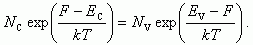
Для
собственного полупроводника уравнение
электронейтральности приобретает вид
p – n = 0
или p = n.
Если ширина запрещенной зоны полупроводника
достаточно велика (Eg
много больше kT)
и если эффективные массы электронов mn
и дырок mp
одного порядка, то уровень Ферми будет
достаточно удален от краев зон
(EC – F > 2kT
и F – EV > 2kT)
и полупроводник будет невырожденным.
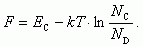
Подставляя
(1.10) и (1.13) в уравнение p + pD – n – nA = 0,
имеем:
![]() . (1.20)
. (1.20)
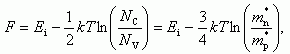
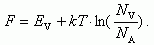
Отсюда
вычисляем F.
Уравнение (1.20) – это уравнение первого
порядка относительно
![]() .
.
Это
дает
 (1.21)
где
через Ei = ½(EV + EC)
обозначена энергия середины запрещенной
зоны. При выводе правого выражения для
F
величина (NC/NV)
была заменена на (mn/mp)
с помощью уравнения (1.11).
Для
случая mn* = mp*
энергия
Ферми в собственном полупроводнике
находится посреди запрещенной зоны
F = (EC + EV)/2.
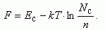
Положение
уровня Ферми зависит от того, какие
другие величины заданы. Если известны
концентрации носителей заряда в зонах
n
и p,
то значение F
можно определить из формул (1.10) и (1.13).
Так, для невырожденного полупроводника
n‑типа
имеем:
![]() . (1.22)
. (1.22)
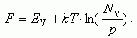
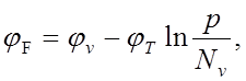
Аналогично
для невырожденного полупроводника
p‑типа
![]() . (1.23)
. (1.23)
Из
выражений (1.22 и 1.23) видно, что чем больше
концентрация основных носителей, тем
ближе уровень Ферми к краю соответствующей
зоны. Для донорного полупроводника
n0 = ND
(1.17), тогда
![]() . (1.24)
. (1.24)
Для
акцепторного полупроводника p0 = NA
(1.19), тогда
![]() . (1.25)
. (1.25)
10. Механизмы рассеяния электронов и дырок
При
рассмотрении движения носителей заряда
в идеальном периодическом
поле кристаллической решетки было
установлено, что электроны
и дырки движутся как свободные частицы.
В
реальном кристалле электроны и дырки
совершают сложные траектории
движения из-за соударений с дефектами
решетки. Поскольку
дефекты, искажающие периодичность поля
решетки и
являющиеся центрами рассеяния, имеют
разную природу, то они будут
обусловливать и различные механизмы
рассеяния носителей заряда.
В
полупроводниках центрами рассеяния
могут быть тепловые колебания
решетки и статические дефекты, такие
как атомы и ионы примеси,
вакансии, дислокации, границы двойников
и кристаллитов. Для
количественной оценки процесса рассеяния
вводится параметр а, называемый
эффективным
сечением рассеяния.
Предположим,
что имеется п
свободных
электронов, которые со
средней тепловой скоростью Vо
движутся
в данном направлении. Тогда
пV0
есть плотность потока электронов, т. е.
количество электронов,
проходящих в единицу времени через
единичную площадку образца,
перпендикулярную направлению их
скорости. Допустим,
что
на пути потока электронов в единичном
сечении образца имеется N
одинаковых центров рассеяния. Каждый
центр характеризуется эффективным
сечением, равным у. Это, по существу, то
пространство вокруг
центра, в области которого имеет место
рассеяние электронов. Поэтому количество
рассеянных электронов в единицу времени
п,
определяется
эффективным сечением у,
количеством
центров рассеяния
N
и
плотностью падающего потока электронов
nV0,
т. е.
n1=уNnV0
(1)
Если
W
— вероятность рассеяния одной частицы
в единицу времени, то количество
рассеянных электронов в единицу времени
п1
есть
n1=Wn
(2)
Тогда
на основании (1) и (2) можно написать
у=n1/NnV0
(3)
Эффективное
сечение рассеяния о есть отношение
числа
электронов, удаленных из пучка в
результате рассеяния на одном центре
в единицу времени, к плотности падающего
пучка частиц.
Эффективное
сечение рассеяния имеет размерность
площади [у]=[W]/[NV0]=T-1/L-3LT-1=L2
(3) Из
формулы (3) найдем, что вероятность
рассеяния
W=уNV0
(4) Следовательно,
вероятность
рассеяния или вероятность столкновения
определяется эффективным сечением,
количеством центров рассеяния
и скоростью движения носителя заряда.
В
то же время вероятность столкновения
обратно пропорциональна
времени свободного пробега:
W=1/ф
(5).
Поэтому
время свободного пробега и длину
свободного пробега можно
выразить через эффективное
сечение.
Из (4) и
(5) следует, что
ф=1/уNV0
(6) или
l=1/уN
Величина
l-1=уN
есть вероятность рассеяния на единичном
интервале
пути. Рассмотрим
случай,
когда имеются различные центры рассеяния.
Пусть
1-й центр характеризуется эффективным
сечением уi,
и число таких
центров равно Ni.
Механизм рассеяния на этих центрах
определяет
длину свободного пробега li.
Если все процессы рассеяния
возможны, то согласно теории вероятности
полная вероятность
рассеяния в единицу времени будет
определяться суммой отдельных
вероятностей рассеяния
W=УWi(8)
Так
как УуiNi
то полная длина свободного пробега
согласно
(4) и (8) может быть определена из соотношения
l-1=Уl-1i
(9)
Согласно
(9) полная
длина свободного пробега всегда меньше
самой
малой парциальной длины свободного
пробега.
Поскольку
роль дефектов в процессе рассеяния
носителей заряда различна,
поэтому различные дефекты должны иметь
разное эффективное
сечение. Для их количественной оценки
за эффективное сечение рассеяния а
примем
площадку, в пределах которой возможно
взаимодействие между носителем заряда
и дефектом.
Такие
дефекты, как вакансии, междуузельные
атомы, во многих отношениях
сходны с примесями замещения. Эти дефекты
называются точечными
дефектами.
Для
них за 0
можно
принять площадь
квадрата со стороной, равной постоянной
решетки, т. е. уА=(5*10-8)2=3*1О-15см2.
Если предположить, что концентрация
атомов примеси NА=1016см-3,
то длина свободного пробега при рассеянии
носителей заряда на атомах примеси
будет составлять lА=(3*10-15*10-16)-1=3*10-2см=300мкм.
Для
иона примеси будем считать, что его
диаметр в 10 раз больше диаметра
примесного центра, т.е. у1=(5*10-8*10)2=3*10-13см2.
В
случае, если N1=1016см-3,
то l1=3*10-4см=3мкм.
Дислокации
являются линейными дефектами,
простирающимися на
большие области кристалла. Предположим,
что линейная дислокация
имеет длину 0,1 см, а ее диаметр измеряется
сотней периодов решетки.
В этом случае площадь ее осевого сечения
равна 5*10-8X100*10-1=5*10-7
см2.
При объемной плотности дислокаций
Nд=108см-3
длина свободного пробега будет порядка
lО=2*10-2см=200мкм.
Границы двойников и кристаллитов, а
также дефекты упаковки представляют
собой двумерные нерегулярности. Они
имеют место в блочных кристаллах и
поликристаллических образцах.
Эффективное
сечение рассеяния на тепловых колебаниях
решетки
определяется S
сечения области, которую занимает
колеблющийся
атом без площади сечения самого атома.
Если
считать, что амплитуда колебаний порядка
r=0,05нм=5*10-9
см, а диаметр атома d
=10-8см,
то уТ=(d+r)2—d2=2rd=10-16см2.
Это значение много меньше, чем для других
центров
рассеяния, но число колеблющихся атомов
велико: NT=1022см-3,
поэтому lT
=
10-6см=0,01
мкм.
Как
оказывается, описание
процессов рассеяния при помощи времени
релаксации возможно, если столкновения
частиц упругие, т. е. такие, при
которых энергия носителя заряда мало
изменяется, и если процессы рассеяния
приводят к случайному распределению
носителей заряда
по скоростям, т. е. имеет место равновероятное
рассеяние носителей
заряда по всем направлениям.
Допустим,
что в момент времени t
=
0 на систему, описываемую неравновесной
функцией распределения f,
перестали действовать внешние
возмущения (выключаются поля) и полевой
член обращается
в нуль. В результате процессов соударений
система придет в
равновесное состояние, описываемое
равновесной функцией распределения
f0.
Это значит, что после выключения внешнего
поля функция
распределения изменяется благодаря
наличию соударений электронов
с дефектами решетки:
df/dt=(df/dt)ст
(1)
В
том случае, когда отклонение распределения
носителей заряда от
равновесного состояния невелико, можно
положить, что в отсутствие
внешних полей скорость изменения функции
распределения вследствие соударений
пропорциональна величине отклонения
функции
от равновесия, т. е. пропорциональна f
— f0:
df/dt=(df/dt)ст=(f-f0)/ф(k)
(2) где
1/ф(к) — коэффициент пропорциональности,
зависящий от к. Решая
уравнения (2), получаем:
f-f0=(f-f0)t=0e—t/ф
(3)
Из
(3) следует, что после
прекращения действия внешних полей
разность (f—f0)
уменьшается
по экспоненциальному закону с постоянной
времени х, которая носит название времени
релаксации. Следовательно,
ф есть
среднее время, в течение которого в
системе существует
неравновесное распределение носителей
заряда после снятия
внешних полей.
Соседние файлы в папке Шпоры
- #
- #
1.6. ����������� ��������� ������ �����
� ���������� ������������ �� �������, ��� ������� ����� �����. ��������� ������, ��� ����� ����� ��������� ������ �����.
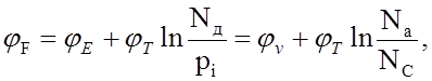
��� ������������ �������������� ��������� �������������������� ����������� ��� p — n = 0 ��� p = n. ���� ������ ����������� ���� �������������� ���������� ������ (Eg ����� ������ kT) � ���� ����������� ����� ���������� mn � ����� mp ������ �������, �� ������� ����� ����� ���������� ������ �� ����� ��� (EC — F > 2kT � F — EV > 2kT) � ������������� ����� �������������.
���������� (1.10) � (1.13) � ��������� p + pD — n — nA = 0, �����:
 (1.20)
������ ��������� F. ��������� (1.20) — ��� ��������� ������� ������� ������������ exp(F/kT).
��� ����
 (1.21)
��� ����� Ei = (1/2)*(EV + EC) ���������� ������� �������� ����������� ����. ��� ������ ������� ��������� ��� F �������� (NC/NV) ���� �������� �� (mn/mp) � ������� ��������� (1.11).
��� ������ mn* = mp* ������� ����� � ����������� �������������� ��������� ������� ����������� ���� F = (EC + EV)/2.
��������� ������ ����� ������� �� ����, ����� ������ �������� ������. ���� �������� ������������ ��������� ������ � ����� n � p, �� �������� F ����� ���������� �� ������ (1.10) � (1.13). ���, ��� �������������� �������������� n-���� �����:
 (1.22)
���������� ��� �������������� �������������� p-����
 (1.23)
�� ��������� (1.22 � 1.23) �����, ��� ��� ������ ������������ �������� ���������, ��� ����� ������� ����� � ���� ��������������� ����. ��� ��������� �������������� n0 = ND (1.17), �����
 (1.24)
��� ������������ �������������� p0 = NA (1.19), �����
 (1.25)
 Постоянство
(“горизонтальность”) уровня Ферми в равновесной системе является одним из
фундаментальных соотношений теории твердого тела. (Сами потоки — дрейфовые и диффузионные могут быть, но
они должны уравновешиваться). Потенциал Ферми для невырожденных полупроводников
определяется выражениями:
(n – типа)
; (8)
(p -типа)
(9)
т.е. у невырожденных полупроводников потенциал Ферми
всегда лежит в запрещенной зоне; (логарифмы в обоих выражениях –
отрицательны!).
С учётом того, что в диапазоне рабочих температур все
донорные атомы ионизированы, можно считать, что
(полупроводник n-типа): n = Nд
, тогда концентрация свободных дырок (pn = ni2)
p = ni2/Nд
.
С учётом приведённого выше
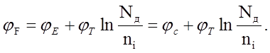
(10)
Отсюда следует, что уровень Ферми в электронном
полупроводнике лежит тем выше, чем больше концентрация доноров и чем ниже
температура.
Для дырочного п/п
P = Na;
n = pi2/Na;
(11)
т. е. уровень Ферми лежит тем ниже, чем больше
концентрация акцепторов и чем ниже температура.
р-слой
n-слой
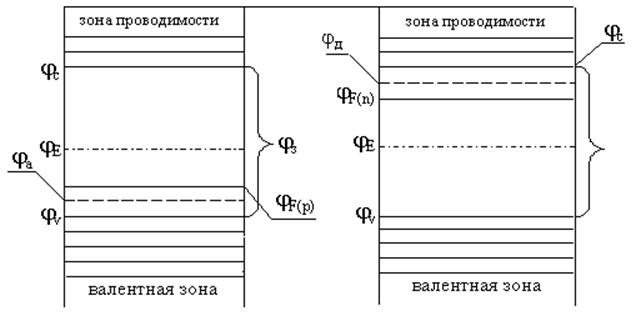
Тогда высота потенциального барьера при контакте p- и n-
слоёв (контактная разность потенциалов):
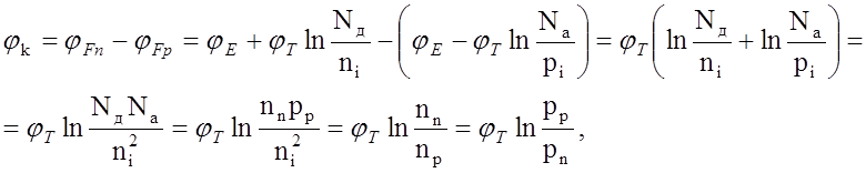
(12)
так как в равновесной системе
уровень Ферми должен быть единым.
Из выражения 12 следует, что контактная разность
потенциалов зависит от температуры и концентрации примесей в слоях p и n (от
степени легирования слоёв).
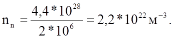
1. Определить
положение уровня Ферми в Ge n – типа при Т = 300 К, если на 2*106 атомов Ge приходится один атом примеси (донорная).
Концентрация атомов в Ge равна 4,4*1028
ат/м3 (N). Постоянная G в выражении, связывающем число электронов в единице объёма в зоне
проводимости с температурой и энергетическими уровнями, равна 4,83*1021
м-3*К-3/2 (Ge). Ширина
запрещённой зоны Ез = 0,72 эВ, а расстояние между дном зоны
проводимости и донорным уровнем 0,01 эВ.
Решение
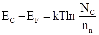
Концентрация электронов в зоне проводимости
определяется выражением
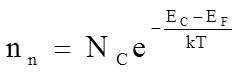 , где (1)
ЕF – энергия уровня Ферми;
ЕС
– энергия нижней границы зоны проводимости;
k – постоянная
Больцмана;
Т
– температура;
NC –
эффективная плотность состояний в зоне проводимости.
В
свою очередь
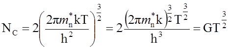 , где (2)
h – постоянная Планка;
![]() — эффективная масса электрона;
— эффективная масса электрона;
G — коэффициент пропорциональности.
Перепишем выражение (1) в виде:
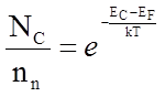 или
или 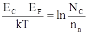 ,
,
откуда
 , (3)
, (3)
что и будем анализировать.
Поскольку концентрация атомов в Ge N =
4,4*1028 м-3 и на 2*106 атомов Ge приходится один атом примеси, а при
температуре 3000 К разница между донорными уровнями и дном
зоны проводимости равна 0,01 эВ при Ед = 0,72 эВ; можно
считать, что все атомы доноров будут ионизированы, тогда число свободных
электронов в нём составит
Эффективная плотность состояний в зоне
проводимости при 3000 К из выражения (2)
 .
.
Из выражения (3) окончательно имеем
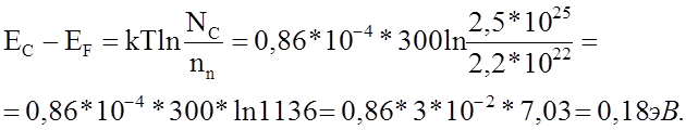
Таким образом, уровень Ферми находится
ниже дна зоны проводимости на 0,18 эВ, что составляет 25 % от ширины
запрещённой зоны.
2. Вычислить
положение уровня Ферми относительно дна зоны проводимости при температуре 4000
К для кристалла Ge, содержащего 5*1022 атомов
сурьмы в м3.
Решение
Сурьма по отношению к германию является донором,
германий будет n-типа, поэтому можно воспользоваться всеми
рассуждениями и математическими выкладками из предыдущей задачи.
Уважаемый посетитель!
Чтобы распечатать файл, скачайте его (в формате Word).
Ссылка на скачивание — внизу страницы.
The Fermi level of a solid-state body is the thermodynamic work required to add one electron to the body. It is a thermodynamic quantity usually denoted by µ or EF[1]
for brevity. The Fermi level does not include the work required to remove the electron from wherever it came from.
A precise understanding of the Fermi level—how it relates to electronic band structure in determining electronic properties, how it relates to the voltage and flow of charge in an electronic circuit—is essential to an understanding of solid-state physics.
In band structure theory, used in solid state physics to analyze the energy levels in a solid, the Fermi level can be considered to be a hypothetical energy level of an electron, such that at thermodynamic equilibrium this energy level would have a 50% probability of being occupied at any given time.[clarification needed]
The position of the Fermi level in relation to the band energy levels is a crucial factor in determining electrical properties.
The Fermi level does not necessarily correspond to an actual energy level (in an insulator the Fermi level lies in the band gap), nor does it require the existence of a band structure.
Nonetheless, the Fermi level is a precisely defined thermodynamic quantity, and differences in Fermi level can be measured simply with a voltmeter.
Voltage measurement[edit]

Sometimes it is said that electric currents are driven by differences in electrostatic potential (Galvani potential), but this is not exactly true.[2]
As a counterexample, multi-material devices such as p–n junctions contain internal electrostatic potential differences at equilibrium, yet without any accompanying net current; if a voltmeter is attached to the junction, one simply measures zero volts.[3]
Clearly, the electrostatic potential is not the only factor influencing the flow of charge in a material—Pauli repulsion, carrier concentration gradients, electromagnetic induction, and thermal effects also play an important role.
In fact, the quantity called voltage as measured in an electronic circuit has a simple relationship to the chemical potential for electrons (Fermi level).
When the leads of a voltmeter are attached to two points in a circuit, the displayed voltage is a measure of the total work transferred when a unit charge is allowed to move from one point to the other.
If a simple wire is connected between two points of differing voltage (forming a short circuit), current will flow from positive to negative voltage, converting the available work into heat.
The Fermi level of a body expresses the work required to add an electron to it, or equally the work obtained by removing an electron.
Therefore, VA − VB, the observed difference in voltage between two points, A and B, in an electronic circuit is exactly related to the corresponding chemical potential difference, µA − µB, in Fermi level by the formula[4]

where −e is the electron charge.
From the above discussion it can be seen that electrons will move from a body of high µ (low voltage) to low µ (high voltage) if a simple path is provided.
This flow of electrons will cause the lower µ to increase (due to charging or other repulsion effects) and likewise cause the higher µ to decrease.
Eventually, µ will settle down to the same value in both bodies.
This leads to an important fact regarding the equilibrium (off) state of an electronic circuit:
This also means that the voltage (measured with a voltmeter) between any two points will be zero, at equilibrium.
Note that thermodynamic equilibrium here requires that the circuit be internally connected and not contain any batteries or other power sources, nor any variations in temperature.
Band structure of solids[edit]


Fermi-Dirac distribution  vs. energy
  , with μ = 0.55 eV and for various temperatures in the range 50 K ≤ T ≤ 375 K.
In the band theory of solids, electrons are considered to occupy a series of bands composed of single-particle energy eigenstates each labelled by ϵ. Although this single particle picture is an approximation, it greatly simplifies the understanding of electronic behaviour and it generally provides correct results when applied correctly.
The Fermi–Dirac distribution, , gives the probability that (at thermodynamic equilibrium) a state having energy ϵ is occupied by an electron:[5]

Here, T is the absolute temperature and kB is the Boltzmann constant. If there is a state at the Fermi level (ϵ = µ), then this state will have a 50% chance of being occupied. The distribution is plotted in the left figure. The closer f is to 1, the higher chance this state is occupied. The closer f is to 0, the higher chance this state is empty.
The location of µ within a material’s band structure is important in determining the electrical behaviour of the material.
- In an insulator, µ lies within a large band gap, far away from any states that are able to carry current.
- In a metal, semimetal or degenerate semiconductor, µ lies within a delocalized band. A large number of states nearby µ are thermally active and readily carry current.
- In an intrinsic or lightly doped semiconductor, µ is close enough to a band edge that there are a dilute number of thermally excited carriers residing near that band edge.
In semiconductors and semimetals the position of µ relative to the band structure can usually be controlled to a significant degree by doping or gating. These controls do not change µ which is fixed by the electrodes, but rather they cause the entire band structure to shift up and down (sometimes also changing the band structure’s shape). For further information about the Fermi levels of semiconductors, see (for example) Sze.[6]
Local conduction band referencing, internal chemical potential and the parameter ζ[edit]
If the symbol ℰ is used to denote an electron energy level measured relative to the energy of the edge of its enclosing band, ϵC, then in general we have ℰ = ϵ – ϵC. We can define a parameter ζ[7] that references the Fermi level with respect to the band edge:

It follows that the Fermi–Dirac distribution function can be written as

The band theory of metals was initially developed by Sommerfeld, from 1927 onwards, who paid great attention to the underlying thermodynamics and statistical mechanics. Confusingly, in some contexts the band-referenced quantity ζ may be called the Fermi level, chemical potential, or electrochemical potential, leading to ambiguity with the globally-referenced Fermi level.
In this article, the terms conduction-band referenced Fermi level or internal chemical potential are used to refer to ζ.

ζ is directly related to the number of active charge carriers as well as their typical kinetic energy, and hence it is directly involved in determining the local properties of the material (such as electrical conductivity).
For this reason it is common to focus on the value of ζ when concentrating on the properties of electrons in a single, homogeneous conductive material.
By analogy to the energy states of a free electron, the ℰ of a state is the kinetic energy of that state and ϵC is its potential energy. With this in mind, the parameter, ζ, could also be labelled the Fermi kinetic energy.
Unlike µ, the parameter, ζ, is not a constant at equilibrium, but rather varies from location to location in a material due to variations in ϵC, which is determined by factors such as material quality and impurities/dopants.
Near the surface of a semiconductor or semimetal, ζ can be strongly controlled by externally applied electric fields, as is done in a field effect transistor. In a multi-band material, ζ may even take on multiple values in a single location.
For example, in a piece of aluminum metal there are two conduction bands crossing the Fermi level (even more bands in other materials);[8] each band has a different edge energy, ϵC, and a different ζ.
The value of ζ at zero temperature is widely known as the Fermi energy, sometimes written ζ0. Confusingly (again), the name Fermi energy sometimes is used to refer to ζ at non-zero temperature.
Temperature out of equilibrium[edit]
The Fermi level, μ, and temperature, T, are well defined constants for a solid-state device in thermodynamic equilibrium situation, such as when it is sitting on the shelf doing nothing. When the device is brought out of equilibrium and put into use, then strictly speaking the Fermi level and temperature are no longer well defined. Fortunately, it is often possible to define a quasi-Fermi level and quasi-temperature for a given location, that accurately describe the occupation of states in terms of a thermal distribution. The device is said to be in quasi-equilibrium when and where such a description is possible.
The quasi-equilibrium approach allows one to build a simple picture of some non-equilibrium effects as the electrical conductivity of a piece of metal (as resulting from a gradient of μ) or its thermal conductivity (as resulting from a gradient in T). The quasi-μ and quasi-T can vary (or not exist at all) in any non-equilibrium situation, such as:
- If the system contains a chemical imbalance (as in a battery).
- If the system is exposed to changing electromagnetic fields (as in capacitors, inductors, and transformers).
- Under illumination from a light-source with a different temperature, such as the sun (as in solar cells),
- When the temperature is not constant within the device (as in thermocouples),
- When the device has been altered, but has not had enough time to re-equilibrate (as in piezoelectric or pyroelectric substances).
In some situations, such as immediately after a material experiences a high-energy laser pulse, the electron distribution cannot be described by any thermal distribution.
One cannot define the quasi-Fermi level or quasi-temperature in this case; the electrons are simply said to be non-thermalized. In less dramatic situations, such as in a solar cell under constant illumination, a quasi-equilibrium description may be possible but requiring the assignment of distinct values of μ and T to different bands (conduction band vs. valence band). Even then, the values of μ and T may jump discontinuously across a material interface (e.g., p–n junction) when a current is being driven, and be ill-defined at the interface itself.
Technicalities[edit]
Terminology problems[edit]
The term Fermi level is mainly used in discussing the solid state physics of electrons in semiconductors, and a precise usage of this term is necessary to describe band diagrams in devices comprising different materials with different levels of doping.
In these contexts, however, one may also see Fermi level used imprecisely to refer to the band-referenced Fermi level, µ − ϵC, called ζ above.
It is common to see scientists and engineers refer to «controlling», «pinning», or «tuning» the Fermi level inside a conductor, when they are in fact describing changes in ϵC due to doping or the field effect.
In fact, thermodynamic equilibrium guarantees that the Fermi level in a conductor is always fixed to be exactly equal to the Fermi level of the electrodes; only the band structure (not the Fermi level) can be changed by doping or the field effect (see also band diagram).
A similar ambiguity exists between the terms, chemical potential and electrochemical potential.
It is also important to note that Fermi level is not necessarily the same thing as Fermi energy.
In the wider context of quantum mechanics, the term Fermi energy usually refers to the maximum kinetic energy of a fermion in an idealized non-interacting, disorder free, zero temperature Fermi gas.
This concept is very theoretical (there is no such thing as a non-interacting Fermi gas, and zero temperature is impossible to achieve). However, it finds some use in approximately describing white dwarfs, neutron stars, atomic nuclei, and electrons in a metal.
On the other hand, in the fields of semiconductor physics and engineering, Fermi energy often is used to refer to the Fermi level described in this article.[9]
Fermi level referencing and the location of zero Fermi level[edit]
Much like the choice of origin in a coordinate system, the zero point of energy can be defined arbitrarily. Observable phenomena only depend on energy differences.
When comparing distinct bodies, however, it is important that they all be consistent in their choice of the location of zero energy, or else nonsensical results will be obtained.
It can therefore be helpful to explicitly name a common point to ensure that different components are in agreement.
On the other hand, if a reference point is inherently ambiguous (such as «the vacuum», see below) it will instead cause more problems.
A practical and well-justified choice of common point is a bulky, physical conductor, such as the electrical ground or earth.
Such a conductor can be considered to be in a good thermodynamic equilibrium and so its µ is well defined.
It provides a reservoir of charge, so that large numbers of electrons may be added or removed without incurring charging effects.
It also has the advantage of being accessible, so that the Fermi level of any other object can be measured simply with a voltmeter.
Why it is not advisable to use «the energy in vacuum» as a reference zero[edit]

When the two metals depicted here are in thermodynamic equilibrium as shown (equal Fermi levels EF), the vacuum electrostatic potential ϕ is not flat due to a difference in work function.
In principle, one might consider using the state of a stationary electron in the vacuum as a reference point for energies.
This approach is not advisable unless one is careful to define exactly where the vacuum is.[10] The problem is that not all points in the vacuum are equivalent.
At thermodynamic equilibrium, it is typical for electrical potential differences of order 1 V to exist in the vacuum (Volta potentials).
The source of this vacuum potential variation is the variation in work function between the different conducting materials exposed to vacuum.
Just outside a conductor, the electrostatic potential depends sensitively on the material, as well as which surface is selected (its crystal orientation, contamination, and other details).
The parameter that gives the best approximation to universality is the Earth-referenced Fermi level suggested above. This also has the advantage that it can be measured with a voltmeter.
Discrete charging effects in small systems[edit]
In cases where the «charging effects» due to a single electron are non-negligible, the above definitions should be clarified. For example, consider a capacitor made of two identical parallel-plates. If the capacitor is uncharged, the Fermi level is the same on both sides, so one might think that it should take no energy to move an electron from one plate to the other. But when the electron has been moved, the capacitor has become (slightly) charged, so this does take a slight amount of energy. In a normal capacitor, this is negligible, but in a nano-scale capacitor it can be more important.
In this case one must be precise about the thermodynamic definition of the chemical potential as well as the state of the device: is it electrically isolated, or is it connected to an electrode?
- When the body is able to exchange electrons and energy with an electrode (reservoir), it is described by the grand canonical ensemble. The value of chemical potential µ can be said to be fixed by the electrode, and the number of electrons N on the body may fluctuate. In this case, the chemical potential of a body is the infinitesimal amount of work needed to increase the average number of electrons by an infinitesimal amount (even though the number of electrons at any time is an integer, the average number varies continuously.):

where F(N, T) is the free energy function of the grand canonical ensemble.
- If the number of electrons in the body is fixed (but the body is still thermally connected to a heat bath), then it is in the canonical ensemble. We can define a «chemical potential» in this case literally as the work required to add one electron to a body that already has exactly N electrons,[11]
where F(N, T) is the free energy function of the canonical ensemble, alternatively,


These chemical potentials are not equivalent, µ ≠ µ′ ≠ µ″, except in the thermodynamic limit. The distinction is important in small systems such as those showing Coulomb blockade.[12]
The parameter, µ, (i.e., in the case where the number of electrons is allowed to fluctuate) remains exactly related to the voltmeter voltage, even in small systems.
To be precise, then, the Fermi level is defined not by a deterministic charging event by one electron charge, but rather a statistical charging event by an infinitesimal fraction of an electron.
Footnotes and references[edit]
- ^ Kittel, Charles. Introduction to Solid State Physics (7th ed.). Wiley.
- ^ Riess, I (1997). «What does a voltmeter measure?». Solid State Ionics. 95 (3–4): 327–328. doi:10.1016/S0167-2738(96)00542-5.
- ^ Sah, Chih-Tang (1991). Fundamentals of Solid-State Electronics. World Scientific. p. 404. ISBN 978-9810206376.
- ^ Datta, Supriyo (2005). Quantum Transport: Atom to Transistor. Cambridge University Press. p. 7. ISBN 9780521631457.
- ^ Kittel, Charles; Herbert Kroemer (1980-01-15). Thermal Physics (2nd ed.). W. H. Freeman. p. 357. ISBN 978-0-7167-1088-2.
- ^ Sze, S. M. (1964). Physics of Semiconductor Devices. Wiley. ISBN 978-0-471-05661-4.
- ^ Sommerfeld, Arnold (1964). Thermodynamics and Statistical Mechanics. Academic Press.
- ^ «3D Fermi Surface Site». Phys.ufl.edu. 1998-05-27. Retrieved 2013-04-22.
- ^ For example: D. Chattopadhyay (2006). Electronics (fundamentals And Applications). ISBN 978-81-224-1780-7. and Balkanski and Wallis (2000-09-01). Semiconductor Physics and Applications. ISBN 978-0-19-851740-5.
- ^ Technically, it is possible to consider the vacuum to be an insulator and in fact its Fermi level is defined if its surroundings are in equilibrium. Typically however the Fermi level is two to five electron volts below the vacuum electrostatic potential energy, depending on the work function of the nearby vacuum wall material. Only at high temperatures will the equilibrium vacuum be populated with a significant number of electrons (this is the basis of thermionic emission).
- ^ Shegelski, Mark R. A. (May 2004). «The chemical potential of an ideal intrinsic semiconductor». American Journal of Physics. 72 (5): 676–678. Bibcode:2004AmJPh..72..676S. doi:10.1119/1.1629090. Archived from the original on 2013-07-03.
- ^ Beenakker, C. W. J. (1991). «Theory of Coulomb-blockade oscillations in the conductance of a quantum dot» (PDF). Physical Review B. 44 (4): 1646–1656. Bibcode:1991PhRvB..44.1646B. doi:10.1103/PhysRevB.44.1646. hdl:1887/3358. PMID 9999698.